")
")
Discrete operational amplifier OPB3
Circuit / Measurement results / Frequency response compensation
There are a large number of integrated operational amplifiers with very good properties available for purchase. However, these also have some fundamental weaknesses. These include problems with high input impedances or small load resistances, i.e. especially at the interfaces of preamplifiers to other components of the audio system. This leads, for example, to the fact that the sound of a CD drive or record player depends not only on the input device itself, but also on the distortion of the preamplifier, which it produces due to the output impedance of the input device. This, of course, causes great problems when optimising the system, as the replacement of a component has hardly manageable effects due to these interactions. The solution is an operational amplifier with an extremely linear input impedance and a potent output stage.
Let's look at two of the problems of many integrated operational amplifiers using the example of an OPA2134.
 |
.png) |
.png) |
The middle diagram shows the dependence of the harmonic distortions on the resistance value Rin for a single, arbitrarily selected OP2134. The measuring frequency is 1kHz, the measuring amplitude 1Vrms. Even relatively small values of Rin, which are quite common in typical audio equipment, lead to a significant increase in harmonic distortion.
The diagram on the right shows the dependence of the harmonic distortions on the load resistance RL. Here, too, a clear increase in harmonic distortion can be seen even at values below 2kOhm. The odd harmonics K3 and K5 are particularly affected. Typical for push-pull amplifiers. Only quiescent current helps here. And this is limited in integrated op's for reasons of power dissipation.
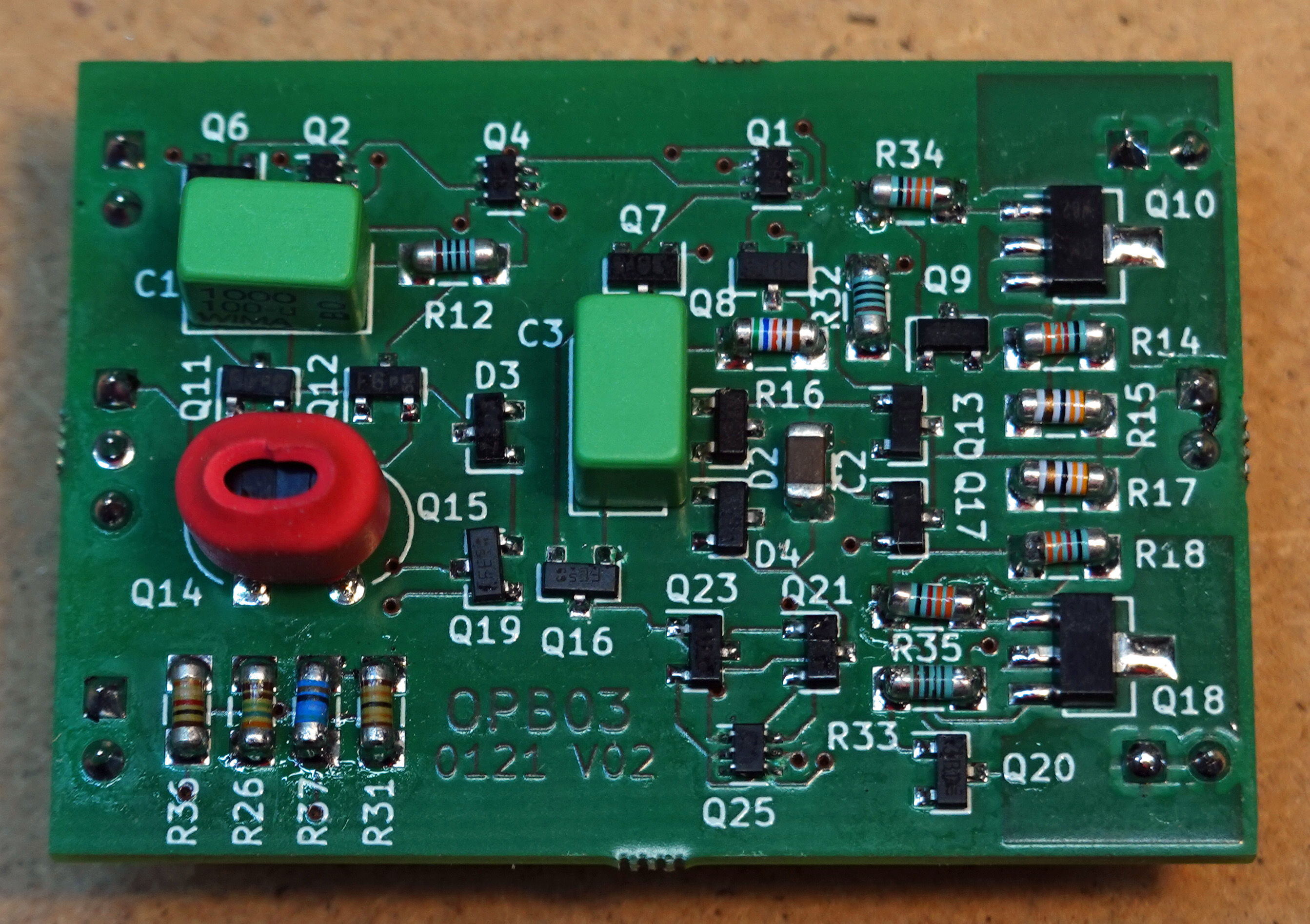
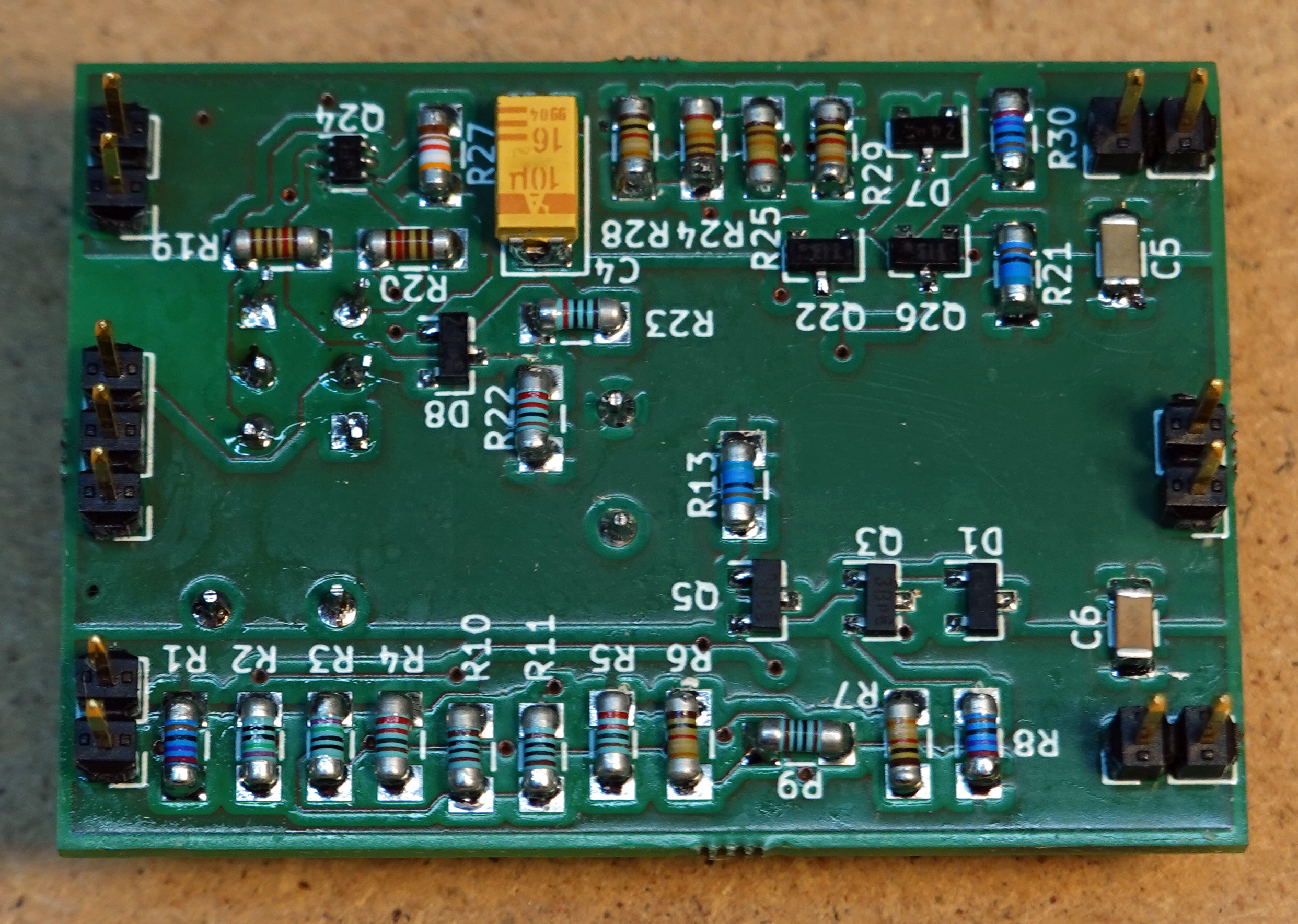
The circuit

The input stage is a classic differential amplifier with matched JFETs on current sources. What is actually special about the input stage is the bootstrapping. With Q19, the common-mode component of the input voltage is tapped and given to the two cascode transistors Q11,Q12 via D3 with an offset of +5.6V. This keeps the drain-source voltage of the input transistors constant. And this also means that the drain-gate capacitance of Q11,Q12 no longer depend on the common-mode voltage. But these are the cause of distortions at high input impedances.
For this purpose, the input stage is massively counter-coupled. I am not a fan of linearisation through extreme over-all negative feedback. I prefer to linearise each individual gain stage largely at the expense of ring gain. In my experience, this leads to really good results.
The input differential stage works on current sources with Q2. The output voltage is fed via the emitter follower Q4 to the second differential amplifier stage. This is also strongly counter-coupled. Via a current mirror Q21,Q23,Q25 the signal voltage goes to a class-A output stage with approx. 20mA quiescent current. At an output voltage of 1Vrms, this is sufficient for load resistors of less than 100 ohms.
 |
 |
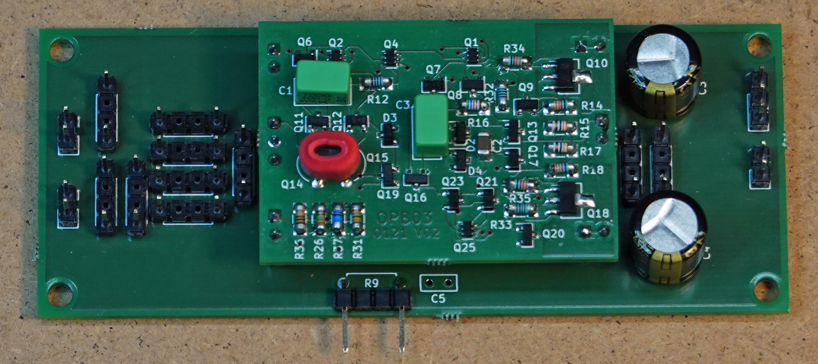
Measurement results
|
OPB3 auf einem Messboard |
.png) |
The harmonic distortion as a function of the input impedance is about 50dB better than our integrated reference within the limits of my measuring accuracy. Only above 100kOhm input impedance does K2 increase slightly. K3-Kx are not detectable with my measuring system and are below -138dB even with an input impedance of 1 MegOhm. The same applies to the harmonic distortion as a function of the load resistance. Here, all harmonics down to a load resistance of 51 ohms are below the measurement limit.
Frequency response compensation
One disadvantage of such a discrete operational amplifier is its limited bandwidth. Passing frequencies of the open-circuit amplification of more than 20MHz, as they can be realised with integrated audio OP's, are compared to up to 3MHz with the OPB3. However, this disadvantage can easily be turned into an advantage by the adjustable frequency response compensation. Due to the discrete design, one is no longer dependent on a universal, 1-pole frequency response compensation, but can adapt it to the special requirements of the respective task. The influencing components are R19/20, R12, C1, R9, C3 and R16. Finding the right combination here certainly requires a little experience, but the result is convincing. Here is an example of an optimised frequency response compensation for an OPB3 as a linear amplifier with 22dB gain. For comparison, I have drawn the no-load gain of an OPA2134. In the lower diagram, the amounts of the no-load gains are shown (red = OP3, blue = OPA2134), above the phase curve.
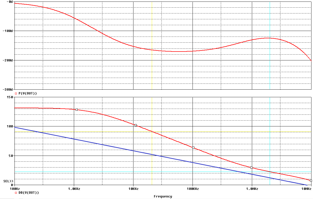
In this example, the open-circuit amplification of the OPB3 is designed as 2-pole and is intercepted to 1-pole shortly before the crossover frequency of the ring amplification at 2MHz. This results in a very good phase reserve of almost 60°. Compared to the OPA2134, the ring gain at 20kHz is approx. 40dB greater. The gain bandwidth product at 20kHz is 400MHz for the OPB3 and 8MHz for the OPA 2134. This is a considerable difference and naturally leads to an extremely low distortion of the OP circuit even in applications with high amplification, such as those required in MM/MC amplifiers.
Here are a few examples of component dimensioning for frequency response compensation
| Ft | Amp | frphase | R19/R20 | R12 | C1 | R9 | R16 | C3 |
| MHz | dB | Ohm | Ohm | pF | Ohm | Ohm | pF | |
| 2 | 0 | 3 | 1200 | 2000 | 120 | 1000 | 120 | 220 |
| 2 | 6 | 3 | 1200 | 2000 | 120 | 1000 | 180 | 150 |
| 2 | 10 | 3 | 1200 | 2000 | 120 | 470 | 270 | 100 |
| 2 | 20 | 3 | 680 | 2000 | 120 | 300 | 560 | 47 |
| 2 | 35 | 3 | 270 | 2000 | 120 | 150 | 560 | 47 |
Download
| Description | Tool | Link |
| PCB manufacturing data | KiCad, Gerber, Excellon | AudioOP3V2_PCB_Gerber.zip |