Characteristic recorder(1)
Sophisticated audio technology also means knowledge of the individual electrical properties of the components used. The characteristic recorder presented here can measure all typical discrete semiconductors under PC control and display complete curves as well as typical characteristic values. It uses a power-compensated pulse measurement method, which keeps thermal errors to a minimum.
If you want to operate sophisticated audio technology, you also have to know your components. And not only according to the data sheet, but also according to the special specimen you want to use. Especially for the pairing of components in some assemblies (differential amplifiers, current mirrors, parallel circuits of power transistors ......) one should be able to measure the characteristics to be paired. Using the example of an input differential amplifier with JFET's I would like to explain this briefly. The properties to be matched are the two control characteristics Id = f(Vgs,Vds). In the simplest case (and I haven't seen anything else yet) the Idss (i.e. Id at Vgs=0 and Vds=fixed voltage) and possibly Vth is measured by both transistors. These are two points from a curve map and the matching is a first approximation, but not perfect yet. If one would record the complete characteristic maps with a suitable curve recorder, one would have many more data points available and could significantly improve the matching. E.g. I typically use two 2SK170 with 2500 data points each. After an evaluation over smallest error squares I can be completely sure, that the two transistors are similar in the whole desired working range.
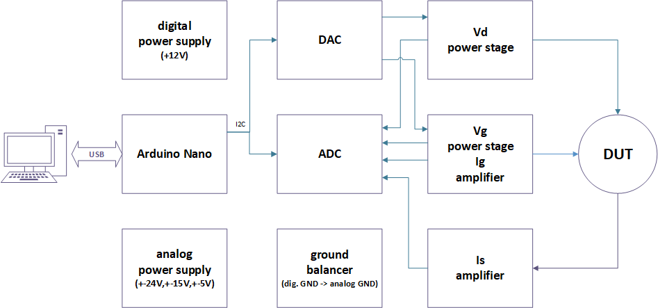
Fig. architecture of the characteristic curve recorder
System circuit diagram with power supply and ground balancer
The architecture of the characteristic curve recorder is converted into a concrete hierarchical block diagram. The ground balancer generates an analog ground of 1/2 Vdd.

DAC / ADC
For the two DAC channels I used inexpensive (ebay ...) modules with 12bit converters in the first step. These output an output voltage from 0 to VDD. This is filtered via the OP's, buffered and converted to GNDA related to +-2.5V. In the layout an extension to own (16bit) DAC's is already planned.
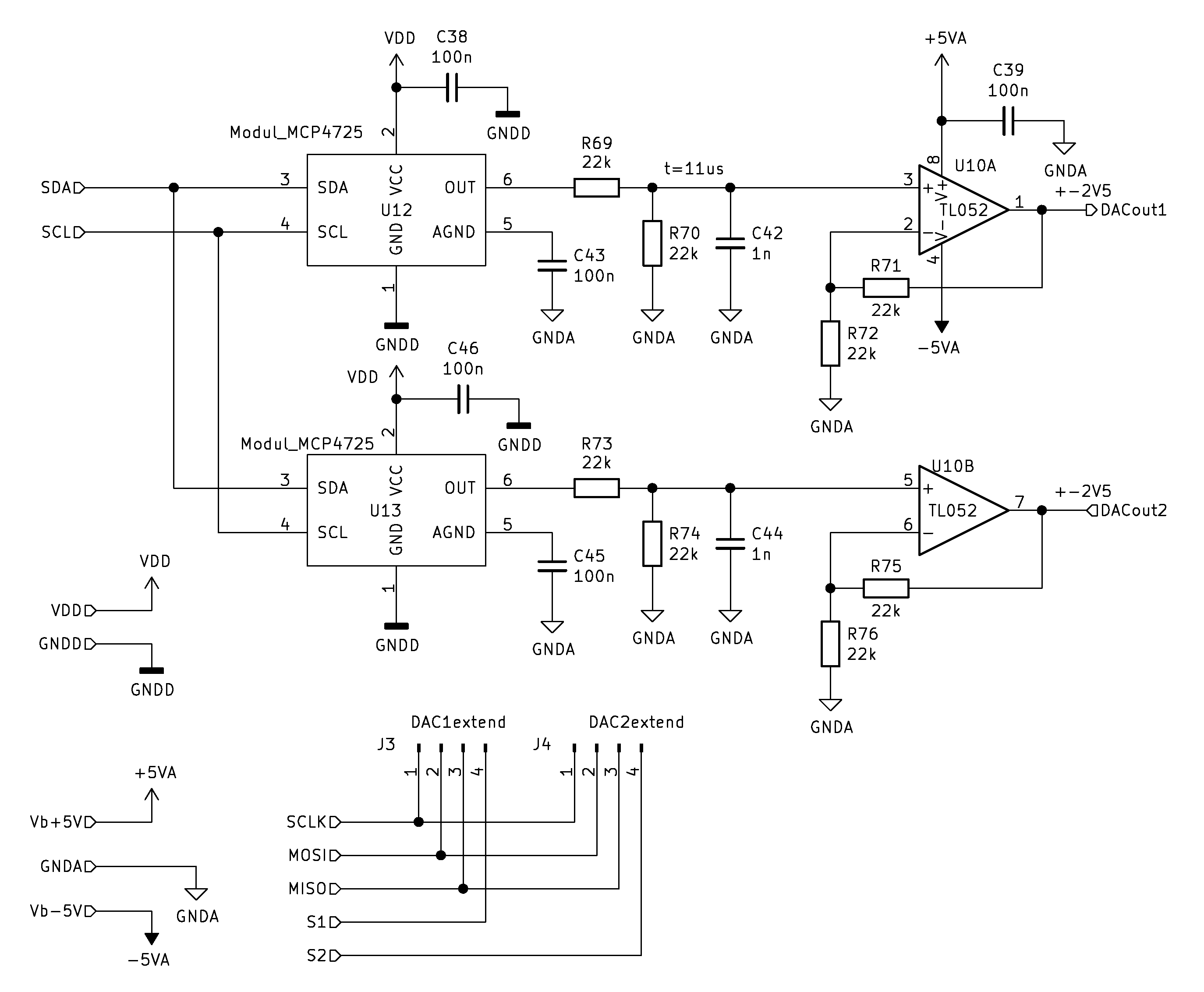
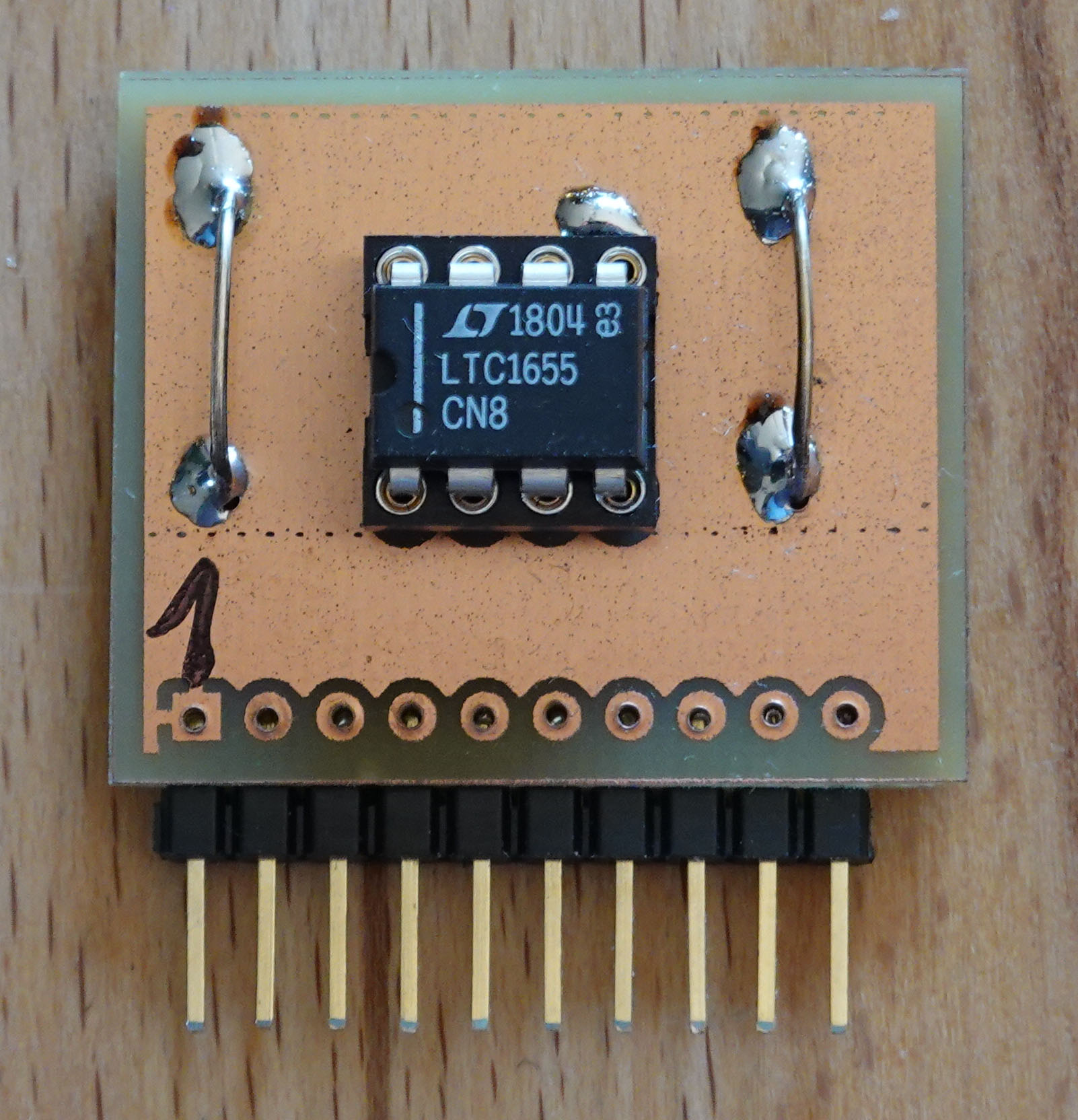
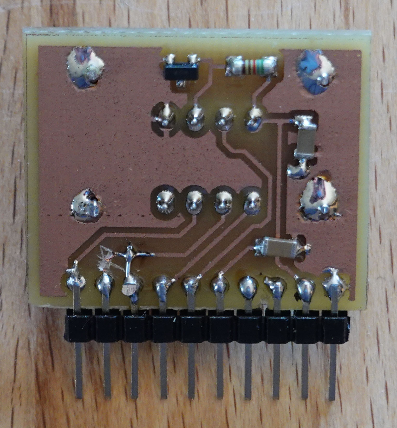
Instead of the MCP4725 modules, 16Bit DAC modules can also be used. These are based on an LTC1655 and operate with an external reference.

 |
|
The 4 required ADC channels are also realized with ready-made modules. The 16bit converters are divided into 2 banks in order to carry out 2 conversions in parallel.

VD Power Stage
The VD power amplifier consists of a high voltage OP LTC2057HV and a power amplifier with 2 complementary Darlingtons. This is sufficient for currents up to 2A and can generate output voltages up to +-25V. The voltage amplification can be switched to x1 or x10 via a relay. At the same time, the scaling of the read-back voltage VDMeasOut is also adapted.

VG Power Stage
Since I wanted to do without regulated, bipolar current sources for the generation of basic currents, I planned a voltage source with switchable series resistors for the control of gate and base. To determine the current I measure the voltage before and after the resistor. Since in addition the measuring ranges of the two voltage measurements can be switched independently of each other, a bandwidth of 100mA results for bipolar transistors up to some nA for gate leakage currents.

Is Amp
The current flowing through our test object is measured as voltage drop via a shunt against ground. In order not to have too great an influence on the voltage of the test object, the shunts are selected with extremely low impedance and operated with a maximum 20mV voltage drop. The measuring range can be selected in 4 steps. 2A, 200mA, 20mA, 2mA at full scale with 16bit resolution should be sufficient for all measurement tasks. The low measuring voltage is then amplified via a chopper-stabilized OP x100 to the measuring range of the AD converters.

data sheet
| min | typ | max | |||
| supply voltage analog | Ub | V | 18 | 24 | 26 |
| supply voltage digital | Ud | V | 10 | 12 | 14 |
| gate/base voltage | Vg | V | -12 | 12 | |
| gate/base current | mA | -120 | 120 | ||
| drain/emitter voltage | Vg | V | -20 | 20 | |
| drain/emitter current | Id | A | -2 | 2 | |
Downloads
| Description | Tool | Link |
| Circuit diagrams | KiCAD, pdf | Prod03_Schaltplan.pdf |
| PCB production data | KiCAD, Gerber, Excellon | KlSr_FABDat_02.zip |
| component placement plan | KiCAD, pdf | Bestückungsplan |
| part list | KiCAD, txt | Kennlinienschreiber_BOM.txt |
| firmware for Arduino | Atmel Studio 7 | HL-Kennlinienschreiber.elf |
| software for Windows | Visual Studio 2019 | publish.zip |
| DAC PCB produnction data | KiCAD, Gerber, Excellon | ModulDAC_LTC1655 PCB Prod V1.02.zip |
Interfacing the DUT
The interfacing of the DUT is quite critical, especially when it is connected via leads and a socket. Depending on the component and the operating point of the measurement, one builds a very high-frequency parasitic oscillator with the DUT, or in combination with the driver stage for UD. Here one must take measures to damp the high frequencies. These should be placed as close as possible to the DUT. Here is an example with which I have had good experience.

Examples of measurement results
Here are some examples of measurement results and their representations. Noticeable are small ripples in the marginal areas of the diagrams. These are caused by the principle of measurement and the mathematical interpolation of the data that is therefore necessary for graphical representation. I originally developed the characteristic curve recorder for matching components. In order to be able to do this optimally in different defined operating point ranges depending on the application, I measure as complete an operating point field as possible from each component. As an example for a 2SK170 Id,Ig = f(Uds,Ugs) with 0<=Uds<=20V, -0.7V<=Ugs<=0.1V with 50 steps each. So in total up to 2500 operating points (Uds,Ugs,Id,Ig). From these data, one can generate any desired representation via corresponding mathematical interpolation. However, due to my limited skills in multidimensional, error-compensating interpolation, small display errors occur. The big advantage of this approach, however, is that with such a data set, future wishes can be fulfilled without having to re-measure the components. This is particularly valuable if, like me, you want to measure 400 2SK170s and later match them in different operating point fields.
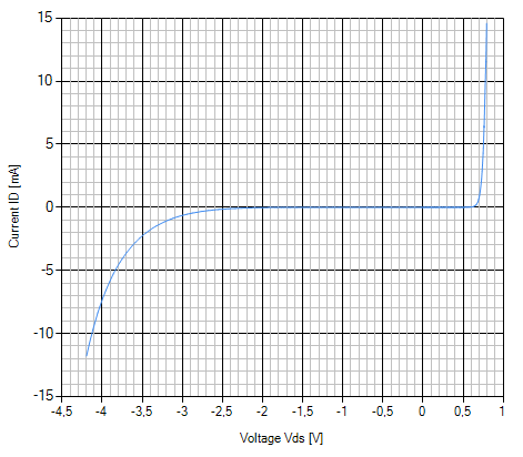 |
Z-Diode v/c diagram |
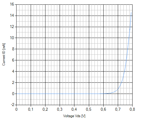 |
Z-Diode v/c diagram |
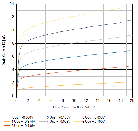 |
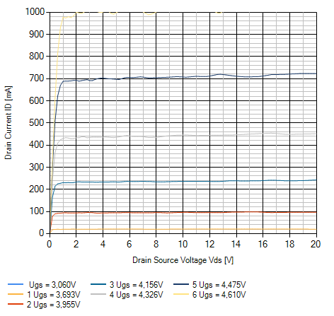
JFET 2SK170 Characteristics diagram |
 |
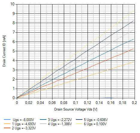
JFET 2SK170 Control characteristics |
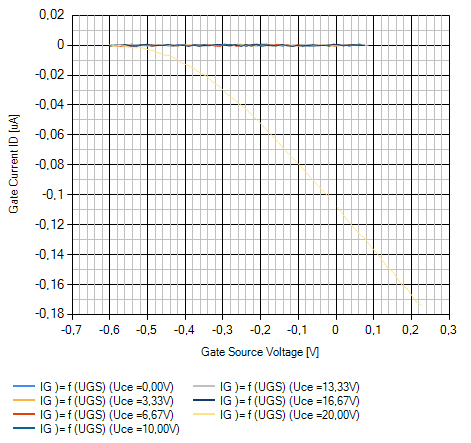 |
JFET 2SK170 Gate leakage current |
 |
JFET J111 ohmic area |
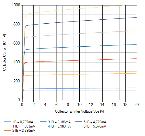 |
BIP BD745 Characteristics diagram |
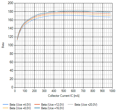 |
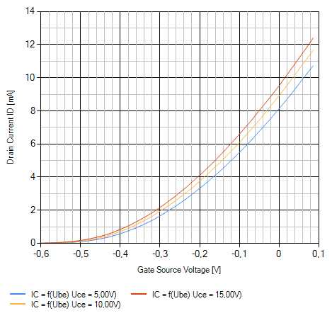
BIP BD745 current gain |
 |
MOSFET IRFP240 Characteristics diagram |
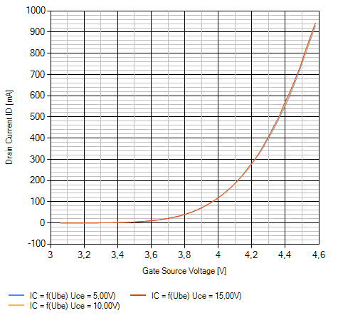 |
MOSFET IRFP240 Control characteristics |
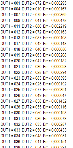 |
automatic matching 100 x 2SK170 best fit |
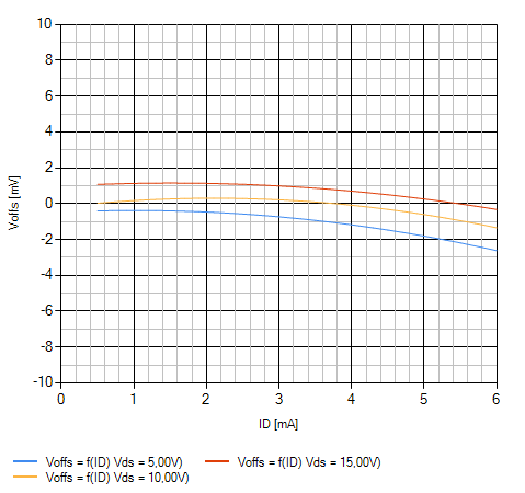 |
Vofs matched pair 2SK170 |
HW changes after .V02 (experimental)
| Nr. | Beschreibung | Grund | Funktionsgruppe | |
| V02.01 | U11 replaces R12 | Improvement of the long-term stability | Balancer | 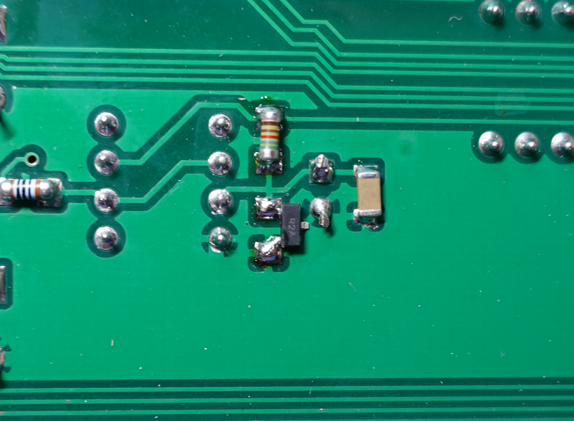 |
| V02.02 | C1 added | Improving stability | VD Power Stage | 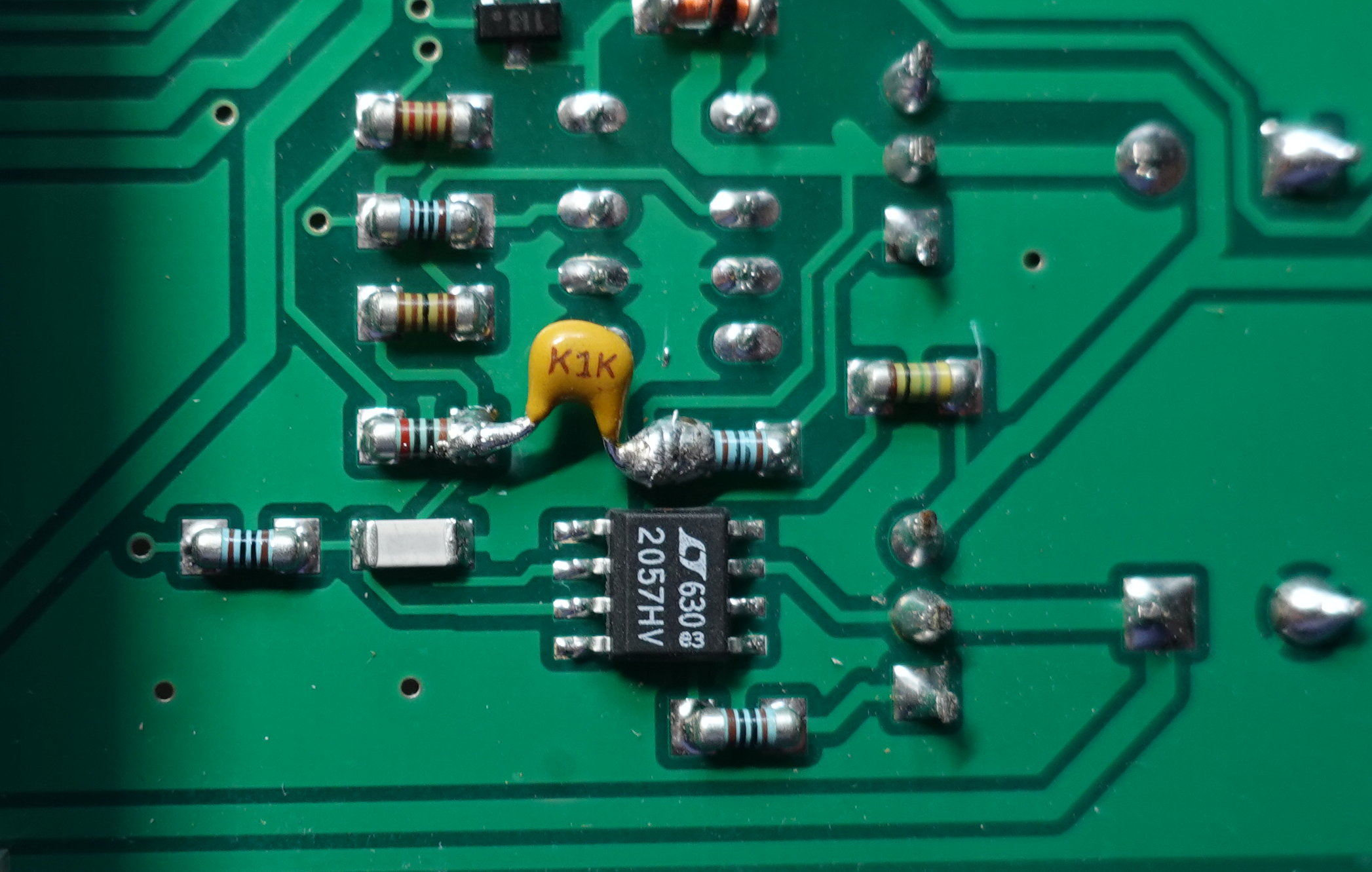 |
| V02.03 | C2 addes | Improving stability | VG Power Stage | 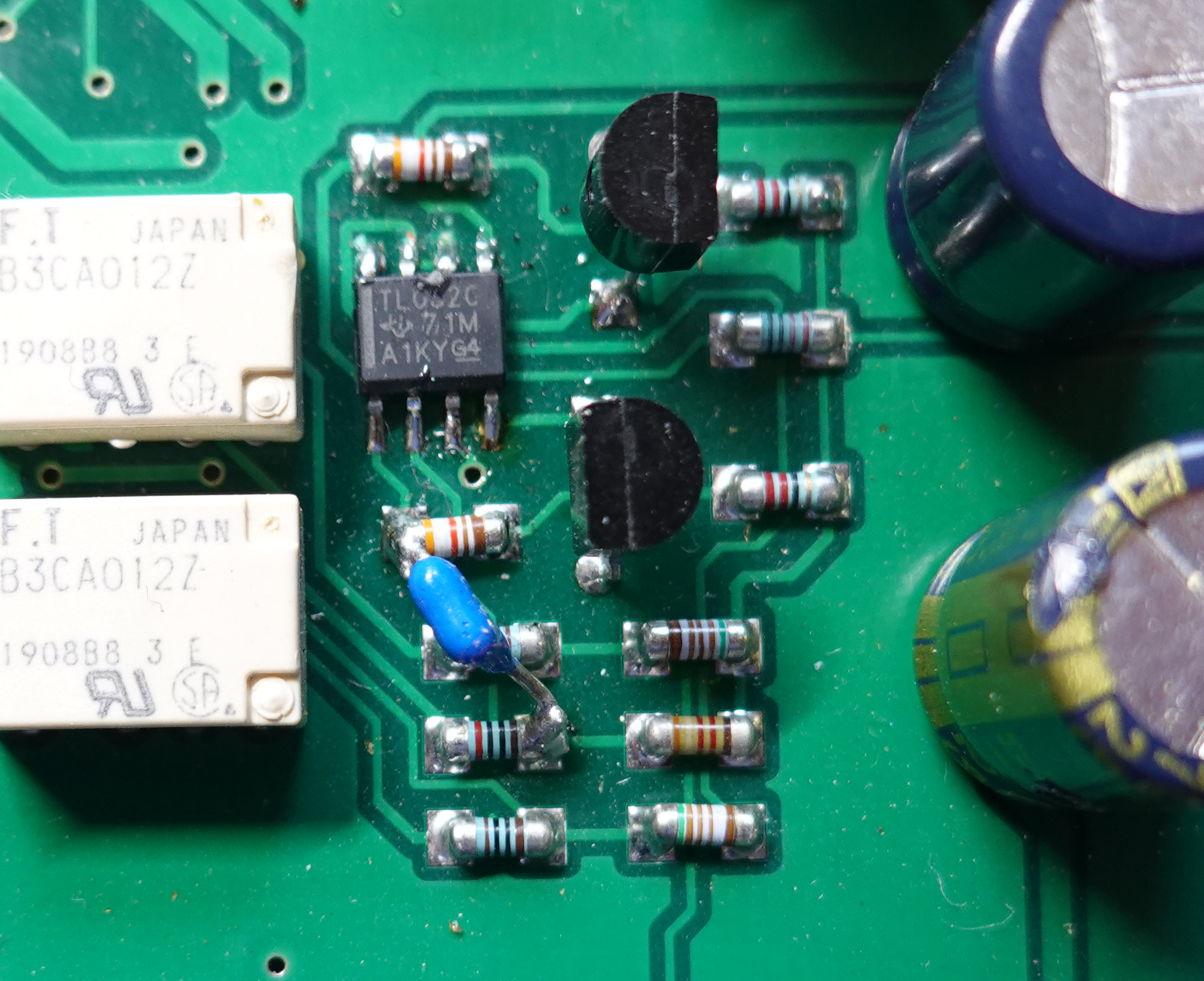 |